I have thought on and off about building a cell-top BMS. Now, contemplating an EV project requiring a 150S BMS, I have been thinking about this some more.
Previous ponderings have dead ended on a communications bus that can handle the common mode voltage differences. There are devices available, but they are generally slow and/or expensive and/or require fixed supply voltages.
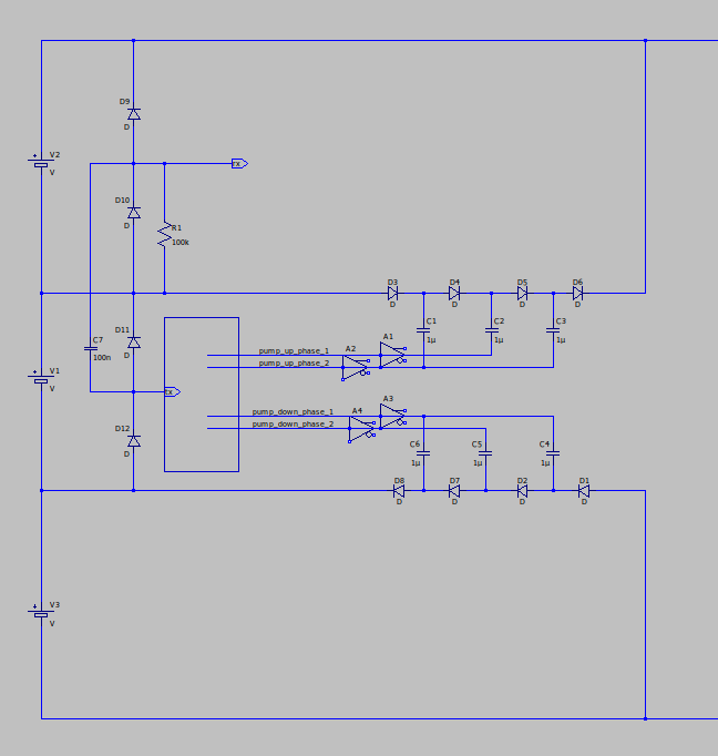
I recently thought about rather chaining devices and using a token passing network. Initially using RS485 transceivers, which are cheap, and can handle some common mode offset. But all the ones I found required fixed supply voltages. Final thought was just straight capacitive coupling:
Only one comms line is shown, but each cell would require 4 (Tx and Rx to the cell above, and the cell below).
The charge pumps can be driven from a DC motor controller (like KA7405D), and should be able to push 1A each to the cells above and below this one.
Using an ATTINY424 processor would allow all the electronics to run directly off the cell voltage, over the full operational range. Total leakage current should be around 2uA, so even though it is permanently connected to the cell, it should take a couple of years for damaging discharge if the pack is not used.
This is still just conceptual/spitballing. It seems way too simple to work as well as simulations say it should, so I am probably missing something…
As someone who likes to re-invent wheels as a hobby and sometimes professionally, I would encourage you to rather go for something like an LTC3300. With balancing, there are a number of pitfalls that are not obvious at the start, but will become very clear later on.
The KA7405D also seems like the wrong choice here - the voltage drops are too much with that BJT based device. Along with those diodes in your charge pump, you might lose more than you gain at each stage…
Once you go to fully integrated solutions, you might as well just buy commercial. Most commercial products are just implementations of the reference design for chips like these. And at R800 for just the basic ICs for 12 cells, it will not be any cheaper to DIY with chips like this.
Discovering and fixing the pitfalls of DIY balancing algorithms will be part of the fun.
It is not ideal. But it will do the job.I have simulated with the datasheet VCEsat, and can still get 1A at 100kHz. It won’t work below 3.2V, but you also don’t want to balance at that point anyway.
I was looking for MOS based drivers, but they are all complex (and expensive) beasties with interal charge pumps to give good gate drive at such low voltage.
At 90c a pop, I can live with the voltage limitations on the KA7405.
I started there, but after days reading datasheets, I came to the conclusion that it just won’t work. High speed opto-couplers are expensive and power hungry. R70 for one opto-coupler vs R2 for 4 diodes and a cap…
Thanks! That DiyBMS project has come a long way since I last looked at it in the V3 days. A lot slicker now, but still quite expensive.
The DRV8837 is also quite nice, and would even let this project work at LTO voltages. But if you don’t need LTO, it will double the board cost for a small increase in efficiency…
Ok, well if you don’t want to go with FET switches, you might as well just make a resistive load, seeing as you are going to be controverting more than half the energy to heat anyway. There is a reason even the capacitive balancers you see on Aliexpress use synchronous FET switching…
Cell top is a different paradigm to bank architecture. With no shared hardware, there are no shared costs. With low supply voltages, switching options are limited.
A charge pump set up will never be efficient (you actually lose more energy in the diodes than even BJT switches). But since the goal is to get rid of energy, that is not really an issue. Getting some of that energy to another cell is a bonus.
You could replace the H-bridge with a more expensive driver, and reduce losses there, but then the diodes would still be a huge loss. So replace them with ideal diodes + controller + separate charge pump supply, and you can finally have efficient energy transfer, but at a ludicrous price.
Can also go simpler with a PWM resistive load - but decent logic level drive trench FETs are not that cheap. So savings are minimal, but might well be worth considering.
But that does bring up an interesting compromise. The same resistive load design with an inductor can create a very simple flyback charger. (Although you would need 2 - one for each direction, and P channel logic level trench FETs are a bit more expensive.)
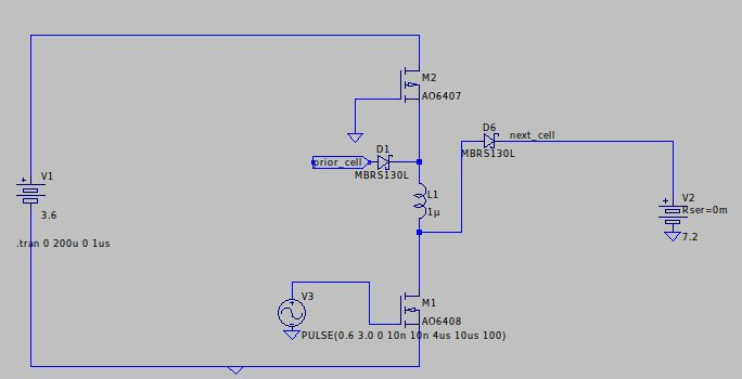
After yesterday’s discussions, I had another look at the balancer.
From the DiyBMS I looked up the switching transistor they used, and it looks like these low voltage high current MOSFETs are no longer unobtanium (last time I looked - a few years ago - they were hard to source, and very expensive).
So something like this is possible:
(To charge the high cell, turn the PMOS on and cycle the NMOS - other way round to charge the low cell).
No need for current sense if you know the inductance (which is easy to calibrate accurately) and you allow the inductor to discharge to 0 current on each cycle. (The trickiest part there is to make sure you are never charging a cell more than one diode drop lower than your own voltage).
Should probably add a decent low ESR cap on the battery side in case the effective inductance of the cell is too high to efficiently charge from pulsed current.
Current is obviously pulsed, which is not great in terms of device utilization, but efficiency is very high and cost is about the same as the charge pump.
EDIT: obviously also missing the gate resistors - this is just a basic functional simulation to test.